LED EDCC Family
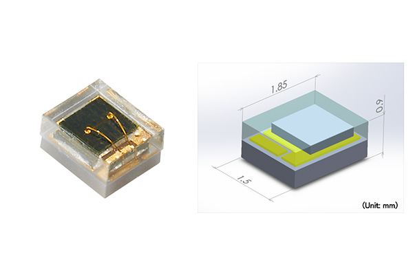
The EDCC Family incorporates traditional high-power LED chips with a wide range of wavelength options, yet it achieves an impressive reduction in footprint of approximately 80% when compared to the previous small-sized EDC Family package. As a result, it offers a compact form factor (W1.5 x L1.85 x H0.9 mm) that closely resembles bare chips and is also compatible with CSP (Chip Scale Package) and other compact-sized packages. This ensures not only ease of customization but also the convenience of handling SMD (Surface Mount Device) packages.
Contact
Key Features
- Utilizes high-power LED chips with a wide wavelength range, including UV, visible light, IR, and SWIR, similar to those used in the SMBB Family and EDC Family
- Compact-sized package, comparable to CSP and high-power LED chips, facilitating easy customization in an SMD-type LED format
- Package design optimized for high-density integration
Applications
- Machine Vision
- Optical Sorting
- Plant Growth
- Security
- Surveillance Cameras
- Optical Authentication
- Inspection Equipment
- Vital Sensing
- and more

Package Design Optimized for High-Density Integration
The EDCC Family features a package design specifically tailored for high-density integration.
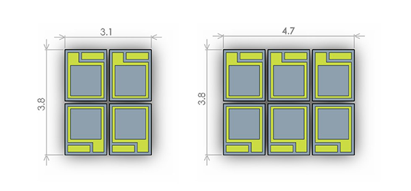
When EDCC packages are arranged in a 2 x 2 configuration, they fit within a compact 4mm x 3.2mm footprint, offering a package size nearly equivalent to the EDC package. Even when arranged in a 2 x 3 configuration, the total footprint remains compact at 4mm x 4.9mm, surpassing the SMBB package in terms of package area efficiency.
| SMBB Flat | EDC Flat | EDCC | |
|---|---|---|---|
| Package area (mm) | 5.0×5.2 | 3.5×3.5 | 1.5×1.85 80% reduction compared to EDC Family |
| Lens type |  |  |  |
 |  |