Surface Treatment
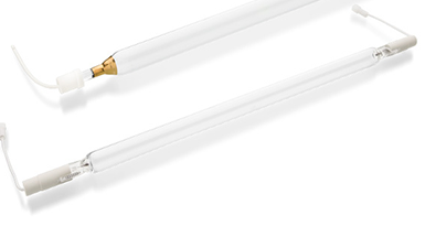
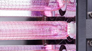
Surface treatment using 172 nm Excimer technology is an advanced process that employs high-energy ultraviolet (UV) light to modify the properties of material surfaces. This technique is highly effective for cleaning, micro-structuring, and enhancing adhesion without causing thermal damage to the substrate.
Industries such as electronics, medical devices, automotive, and aerospace benefit from Excimer technology due to its precision, efficiency, and ability to treat delicate materials. By providing uniform and controlled surface modification, Excimer technology ensures high-quality results, supporting the production of superior, high-performance products.
Excimer vs. plasma and corona: cool efficiency
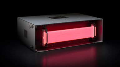
Compared to conventional processes such as plasma and corona, excimer technology is characterized by its low heat emission - it is considered a “cold” radiation source. This means that even sensitive materials such as monofoils can be treated without thermal stress. Excimer treatment offers decisive advantages, particularly in the display and semiconductor industry, sensor technology and in the production of printed electronics and batteries:
- Gentle surface treatment without structural changes
- Uniform activation through photon-supported processes
- Improved adhesion and optimized surface tension
Surface Cleaning: Renoving production-related contaminents
Surface cleaning is an essential intermediate production step in most industrial applications to remove production-related contaminants from surfaces.
In excimer surface cleaning, the material to be cleaned is irradiated with short-wave VUV (Vacuum Ultra Violet) light with a wavelength of 172 nm. Due to the high photon energy of 7.2 eV, organic substances such as dust, fats and oils, as well as oxide layers in some cases, can be broken up and disintegrated into molecular fragments.
During this process, ozone is generated in the air film between the excimer module and the material, which oxidizes and dissolves molecular fragments. The result is a clean surface.
Surface activation: For optimised bonding properties
Surface activation is the process by which a layer with better bonding properties is exposed on the surface of substrates (glass, metal and plastics). This significantly increases the printability, coatability and bondability of the substrates.Surface activation leads to a measurable increase in quality, especially in industrial applications such as printing, coating and bonding.
Surface activation uses 172 nm excimer radiation to remove impurities or passivation layers while simultaneously forming electronegative molecular groups. This combination leads to an increase in surface energy, also called surface tension. Surface tension defines the quality of wettability. It is measured via the contact angle between the surface and the liquid (inks, coatings, adhesives) and can be determined with the aid of test inks, for example: the smaller the contact angle between the liquid and the surface of the substrate to be wetted, the better the adhesion, the clearer the printed image, the more brilliant the colors, etc. The surface tension is determined by the surface of the liquid.
Adhesive based joining: Improved adhesion
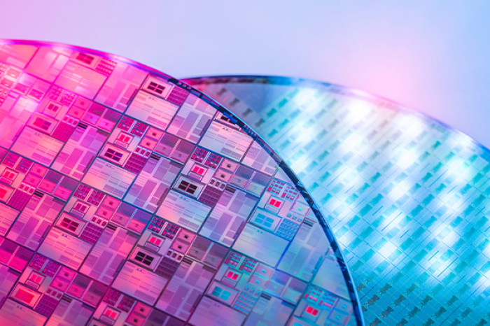
Among the various joining techniques, adhesive-based joining of components is becoming increasingly popular. The decisive factor for good bonding is the adhesion of the adhesive to the surfaces to be bonded. Especially with plastic, metal and glass surfaces, good adhesion is not inherent. By means of pretreatment using excimer technology, the adhesion of adhesives to surfaces is greatly increased. The pretreatment step is gentle, uniform and cold and leaves no surface defects. Typical applications are found wherever large areas have to be bonded, e.g. when bonding films, components in the automotive sector or when joining two wafers in the semiconductor industry.
Optical bonding: Precise, resistant joints
A special variant of adhesive-based bonding is optical bonding, in which a full-surface, transparent adhesive bond is produced by means of a liquid adhesive (LOCA process). This process is used to bond the display, touch sensor and cover glass together in the course of manufacturing display solutions, which offers several advantages:
Color brilliance and contrast of the display solutions are significantly increased because filling the gap between the various display elements with adhesive reduces annoying reflections. In addition, the adhesive layer between the layers increases resistance to mechanical influences such as impacts and shocks.
However, all this can only be achieved if the adhesive adheres perfectly to the surfaces and bonds them permanently and stably. To ensure this, the surfaces can be pretreated with excimer irradiation during the manufacturing process. In this process, the surfaces are activated on the basis of radiation, which leads to homogeneous and optimized adhesion properties of the adhesive.
Photobonding: Adhesive-free connections
The lesser-known process of excimer-assisted photobonding is also used to join two surfaces, but is a completely adhesive-free and heat-free alternative. It uses radiation-based surface activation to allow two surfaces to be bonded together with low pressure. This process is particularly suitable for joining materials with optical functions, such as silicone, glass, PDMS, PC, PMMA or COP, i.e. materials with a high optical surface quality that must be maintained, or interfaces that must not contain foreign substances (such as adhesives).
Excimer-based optical bonding is therefore ideal for manufacturing processes of sensors, components with optical function, biomedical components (lab-on-chip), displays and photovoltaic components.
Are you interested in excimer technology?
Let's find out together how 172 nm excimer technology can improve your production processes. Our team of experts will provide you with comprehensive advice - from the initial concept idea to practical implementation.
Your benefits with Ushio:
- Expert advice from our engineers
- Individual project design and material analysis
- Test laboratory in Germany for practical tests
- Flexible testing options directly at your site
Contact us today and let us work together to find the optimum solution for your requirements.
contact us